

Ultrasonic Water Level Measurement System / LabVIEW Host Computer Interface Editing DIY Bulk Module Circuit Board | Инструменты
Сохраните в закладки:


История цены
*История изменения цены! Указанная стоимость возможно, уже изменилось. Проверить текущую цену - >
| Месяц | Минимальная цена | Макс. стоимость | Цена |
|---|---|---|---|
| Feb-21-2026 | 5554.89 руб. | 5665.54 руб. | 5609.5 руб. |
| Jan-21-2026 | 4504.74 руб. | 4594.76 руб. | 4549 руб. |
| Dec-21-2025 | 5466.8 руб. | 5575.96 руб. | 5520.5 руб. |
| Nov-21-2025 | 5423.94 руб. | 5531.54 руб. | 5477 руб. |
| Oct-21-2025 | 4329.23 руб. | 4416.0 руб. | 4372.5 руб. |
| Sep-21-2025 | 5335.16 руб. | 5442.53 руб. | 5388.5 руб. |
| Aug-21-2025 | 5291.75 руб. | 5397.28 руб. | 5344 руб. |
| Jul-21-2025 | 5248.95 руб. | 5353.89 руб. | 5300.5 руб. |
Новые товары
КОМПЛЕКТ НАКЛЕЕК E30 E40 E60 2 ТАКТ 30 л.с. 40 л.с. 60 л.с. ENDURO OUTBOARDS ДВИГАТЕЛЬ ДЛЯ МОТОРНОГО КАТЕРА МОРСКАЯ ДЕКОРАЦИЯ.
2165.62

Лента Тканевая Обтекательная Катушка с Креплением Зажимом для Обметывания Машины Шитья Аксессуары.
Экскаватор Komatsu 130/200/220/300/360-7, блок внешней ручки замка двери кабины и внутренний.
4132.8
Автомат для оплаты кредитной картой в столовой Sony Canteen, подключенный к сети автоматических торговых аппаратов для приема питания.

Многофункциональная Оловянная стальная сетка для растений материнской платы

Универсальный набор для снятия и установки распределительной цепи мотоцикла для ATV, квадроцикла, грязевого и мотоцикла мотокросса и мотарда.

10 шт. большие петли для распределительного шкафа | Детали инструментов AliExpress

Защита при торговле мотором Poclain MS05 MS18 MS25 MS35 MS50 MS83, серия MS18-1-111, MS11-2-121-F11-1120-000 Гидравлический поршень.
327085.7
Характеристики
Ultrasonic Water Level Measurement System / LabVIEW Host Computer Interface Editing DIY Bulk Module Circuit Board | Инструменты
Описание товара
modname=ckeditor
\
\
\
\
\
\
\
\
\
\
\
\
\
\
\
\
\
\
\
\
\
\
\
\
\
\
utilizeLabview2017Complete the ultrasonic water level measurement system。(20branch)\
\
\
\
\
\
\
\
\
\
\
\
\
\
\
\
\
\
\
\
\
\
\
\
\
\
\
\
\
\
\
\
\
\
\
\
\
\
\
\
\
\
\
\
\
\
\
\
\
\
\
\
\
\
\
\
\
\
Player inDCreate a folder under the root directory。Folder name isAD+Station number。\
\
\
\
\
utilizeDThe reference file in the disk reference file directory generates its own library file。(2branch)\
In your own symbol library and encapsulation Library,DesignFJ5161AH、74LVC1G80、74AHC1G00Symbols and encapsulation of(2branch)。\
FJ3461AHBoth symbol and package names areLED8x1,4LVC1G80and74AHC1G00The package name isSOT-23-5A。\
Use your own symbol library,Draw schematic diagram,As shown in the figure3Shown。(3branch)\
\
\
\
\
According to the circuit schematic diagram completed by the design,DesignPCBPrinted circuit board diagram。(8branch)\
\
\
\
\
\
\
\
\
\
\
\
'
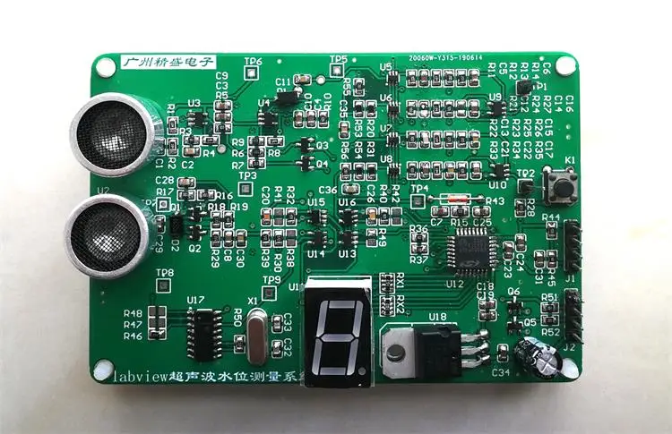
Product name:Ultrasonic water level measurement system/labviewUpper computer interface editing/DIYSpare parts
\\
Product model: JSD-CSBSW
\\
product price :240element
\\
\
\
Jiangsu Vocational School skills competition
\\
Electronic circuit assembly and adjustment and Application
\\
project assignment paper-National competition training
\\
\
\
Competitor station number
\\
_________________________________________________________________________
\\
Work tasks and requirements
\\
Please stay here4Within hours,Complete three parts of work tasks,Specific tasks and requirementsas follows:
\\
1.Complete the assembly of ultrasonic ranging circuit、Testing and commissioning。
\\
2.utilizeLabview2017The control interface of ultrasonic water level measurement system is completed,Realize the test and evaluation of on-site sample paper;Using data collectormyDAQComplete the specified data collection。
\\
3.utilizeAltium Designer10The software completes the PCB design of the specified circuit。
\\
Total score full score70branch。
\\
\
\
\
\
Above tasks,In addition to live works,Please record the rest on the computerDUnder the root directory,“Z+Station number work”In folder,Include answer sheet documents。The blank answer sheet document is in theDDisk reference folder。
\\
Task 1 Ultrasonic ranging circuitAssembly of、Testing and commissioning (30branch)
\\
According to the figure5Schematic diagram shown、chart4Assembly drawings and tables shown2List of components shown,Correctly select components,Accurately welded to the printed circuit board provided by the stadium。
\\
Welding requirements:The solder joint size of electronic components welded on the printed circuit board is moderate、smooth、Mellow、clean,No burr;Correct position;passionless、false、empty、Continuous welding。The pin processing size and forming meet the process requirements,Conductor length、The length of wire stripping head shall meet the process requirements,The core wire is intact,Tinning of twisting head。Including:SMD component welding and in-line component welding。
\\
Assembly requirements:Welding and installation of components without errors and omissions;The plug-in position on the circuit board is correct,Connector、The fasteners shall be installed reliably and firmly;components and parts、The installation of wires and the direction of character marks on components shall meet the process requirements;The circuit board and components shall be free of burns and scratches,The whole machine is clean and free of dirt。
\\

\
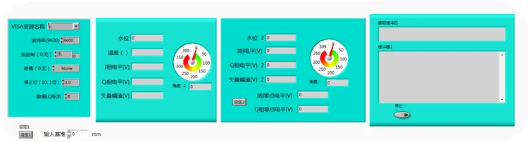
Task 2 Making of system control interface(25branch)
\\
\
utilizeLabview2017Complete the ultrasonic water level measurement system。(20branch)\
\
\
\
\
\
\
\
\
\
\
\
\
\
\
\
\
\
\
\
\
\
\
\
\
\
\
\
\
\
\
\
\
\
\
\
receive data
\\
meaning
\\
M[0]I0=1.096V.Q0=1.084V. 00:08
\\
pattern0,IPhase level1.096V,QPhase level1.084V,Power on time00branch08second
\\
M[1]I1= 0.068V. Q1= 0.019V. V1= 0.071V. A1= 015. 00:27
\\
pattern1,IPhase level0.068V,QPhase level0.019V, Vector amplitude0.071V,angle15degree,Power on time00branch27second
\\
M[2]I2= 0.127V. Q2= 0.097V. V2= 0.160V. A2= 037. 01:11
\\
pattern2,IPhase level0.127V,QPhase level0.097V,Vector amplitude0.160V,angle37degree,Power on time01branch11second。
\\
M[3]T0:25.29C 01:14
\\
pattern3,25.29centigrade,Power on time01branch14second
\\
M[4]V1=0.187V.A1= 037 01:17
\\
pattern4,Vector amplitude0.187V,angle37degree,Power on time01branch17second
\\
M[5]V2=0.049V.A2= 026 02:58
\\
pattern5,Vector amplitude0.049V.,angle26degree,Power on time02branch58second
\\
\
surface1 Serial communication protocol
\\

\
\
\
\
\
Task three Printed circuit board design(15branch)
\\
requirement:
\\
\
Player inDCreate a folder under the root directory。Folder name isAD+Station number。\
\
\
All circuit board design files of the contestant are saved in this folder。
\\
\
utilizeDThe reference file in the disk reference file directory generates its own library file。(2branch)\
In your own symbol library and encapsulation Library,DesignFJ5161AH、74LVC1G80、74AHC1G00Symbols and encapsulation of(2branch)。\
FJ3461AHBoth symbol and package names areLED8x1,4LVC1G80and74AHC1G00The package name isSOT-23-5A。\
Use your own symbol library,Draw schematic diagram,As shown in the figure3Shown。(3branch)\
\
\
requirement:Indicate your station number below the schematic diagram。
\\
\
According to the circuit schematic diagram completed by the design,DesignPCBPrinted circuit board diagram。(8branch)\
\
\
requirement:
\\
(1)Draw the physical boundary of the circuit board on the mechanical layer,size:50mm×80mm。
\\
(2)Dimensions of four fixing holes;aperture3.2mm,Distance between hole center and plate edge2.5mm。
\\
(3)The nixie tube is arranged at the upper left of the circuit board,Its boundary is separated from the upper and left sides2.5mm±0.2mm。
\\
(4)General wiring clearance0.2mm。Wiring lineweight0.25mm,Power line width0.4mm。
\\
(5)Teardrop on all components。
\\
(6)Double side copper clad grounding,Copper clad gap0.5mm。
\\
(7)Indicate your station number on the outside of the upper part of the circuit board。
\\
\
\
\
'
Трекер стоимости
Отзывы покупателей
Новые отзывы о товарах

Евгения Викторовна Макотрина 21 Декабря 2021, 12:15 #
Удобный и функциональный чехол-книжка из высококачественно� � эко-кожи надёжно защитит корпус Вашего смартфона, облада ющего высокой износостойкостью, морозоустойчивост� �ю, а также,... Читать отзыв полностью...

Анна 23 Декабря 2021, 13:49 #
Заказала такое красивенькое платье яркого розового цвета на рост 110 см с пышной юбкой, что пришита внизу... Читать отзыв полностью...

Мария 18 Декабря 2021, 17:25 #
Искала что-то такое цвета а-ля Барби. А тут еще и серебристая оторочка, и блейзер выглядит совсем гламурно. Подкладка с розами... Читать отзыв полностью...

Нина 18 Декабря 2021, 21:12 #
Мозаика пришла быстро, в надёжной упаковке и без посторонних запахов. С удовольствием с ребёнком провели время, собирая эту картину, ну... Читать отзыв полностью...

Виктория 18 Декабря 2021, 19:19 #
Заказала две оригинальные устойчивые удобные подставки для книг в форме кактуса, изготовленные из чугуна. Теперь на моем письменном столе полный... Читать отзыв полностью...

Оксана 23 Декабря 2021, 13:57 #
Моя дочка давно мечтала о красивом красном платье на праздники. Я ей решила заказать и подарить такое нарядное платье ей... Читать отзыв полностью...

Блин это шедевр современной литературы, Что-то наподобие метро и старых супергероев. Я очень рад, что прочитал данный роман и желаю... Читать отзыв полностью...